
(or clock cycles) needed to
fetch and execute a typical instruction. When a data-path supports many
simultaneous transfers among data-path elements, the control unit requires
fewer states (and clock cycles) to execute a given
instruction.(Ri , Rj):
Figure 11.8 shows how this can be implemented for the four-register example
using 4-to-1 multi-plexers.
Each of the four registers receives its parallel load
inputs from an associated multiplexer block. Ri is an edge-triggered
register, which is loaded when the LDi input is asserted. We assume the
load signal takes effect only on the appropriate clock edge; that is, it
is a synchronous control signal. If each register is N bits wide,
the multiplexer blocks must contain N 4-to-1 multiplexers, one
multiplexer for each bit in the register. These are controlled by the 2-bit-wide
selection inputs, Si<1:0> for register Ri.
Register Transfer Operations and Event Timings To
see some of the possible transfers and how they may be implemented, consider
the register transfers R1 --> R0 (transfer
the contents of R1 to R0) and R2
--> R3 (transfer the contents of R2 to
R3). The following detailed register transfer operations
describe the necessary sequencing of the control signals:
01 --> S0<1:0>;
10 --> S3<1:0>;
1 --> LD0;
1 --> LD3;

Figure 11.9 shows a state diagram fragment to illustrate when the control
signals are asserted and when they take effect. We assume a Moore machine
implementation (a synchronous Mealy with registered outputs
behaves analogously). When entering state X the multiplexer
control signals are asserted, gating R1 and R2 to the
inputs of R0 and R3. The state also asserts the R0
and R3 load signals. But because these are synchronous, they do
not take effect until the next state transition.
Thus, the R1 and R2 signals have time
to propagate through the multiplexer blocks and become stable for the requisite
setup times before the clock edge arrives that advances the finite state
machine to state Y. The contents of R0 and R3
change on this state transition, not the one that caused the load inputs
to become asserted. Since the new values take some time to propagate through
the register load circuitry before they emerge at the outputs, the hold
time requirements at the register inputs are easily met.
The SWAP Operation To see how the
interconnection scheme can implement a SWAP operation, you need to understand
the timing relationship between register transfer operations and their effect
on the data-path. Consider a SWAP between registers R1 and R2.
The control signal settings are
01 --> S2<1:0>;
10 --> S1<1:0>;
1 --> LD2;
1 --> LD1;
Discussion The point-to-point
scheme is so flexible that it can transfer new values into the four registers
at the same time. But there is a significant hardware cost. A 4-to-1 multiplexer
requires at least five gates for its implementation (recall
Figure 4.29). Assuming a 32-bit-wide data-path, this means
160 gates per register or 640 gates for the four-register example. For this
reason, point-to-point connections can only be used in rare cases in which
the flexibility far outweighs the implementation cost.
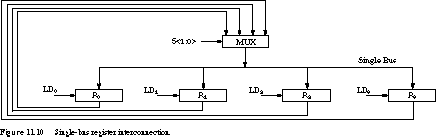
The block with a multiplexer for each register has been replaced by a block with a single multiplexer that is shared by all registers. The hardware cost is 25% of that of the point-to-point approach. The multiplexer places selected data on a bus that feeds the load inputs of all registers.
This dramatic reduction in hardware cost comes at a
price: The shared bus (and its multiplexer) is
a critical resource because it can be used by only one transfer
at a time. However, the single source register can still "broadcast"
simultaneously to more than one destination register.
The Register Transfers Revisited To
see that transfers now require more states, let's again consider the transfer
of R1 to R0 and R2 to R3. These now
require two separate states, asserting the following control signals:
State X:(R1 --> R0)
01 --> S<1:0>;
1 --> LD0;
State Y:(R2 --> R3)10 --> S<1:0>;
1 --> LD3;
State X:(R1 --> R4)
001 --> S<2:0>;
1 --> LD4;
State Y:(R2 --> R1)
010 --> S<2:0>;
1 --> LD1;
State Z:(R4 --> R2)
100 --> S<2:0>;
1 --> LD2;
(we assume one clock
cycle per state). Using a single bus interconnection, however,
SWAP requires an extra register, a larger MUX, and three control states.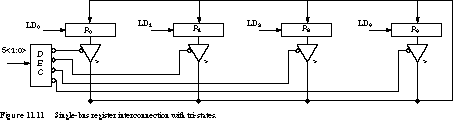
Any of the four registers can be the source for the single bus or be loaded from it. The decoder guarantees that only one of the registers is gated onto the bus through its tri-state buffers. Most packaged logic registers include tri-state devices, so this form of interconnection is convenient.
(and clock cycles) it takes
to implement a simple instruction.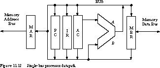
Figure 11.12 gives a simple single-bus design for the processor described in Figure 11.4. The registers are MAR, MBR, PC, IR, and AC, and the only functional unit is the ALU. The AC is hardwired to the A input of the ALU and the MAR is write-only. We call this figure a register transfer diagram because it highlights the way registers and functional units are interconnected.
By examining the data-path, we can quickly determine
the register transfer operations it supports:
[X]"
which adds the contents of memory location X to the AC and stores
the result back into the AC. With the connection scheme of Figure 11.12,
the set of register transfer steps to execute the instruction are the following
(we group the operations by state and cycle):Multiple Bus Register Transfer Diagram

Figure 11.13 gives an alternative three-bus organization that supports
higher parallelism in the data-path. More parallelism means that more transfers
can take place in the same state. This should lead us to a reduced state
and cycle count for the typical instruction.
We partition the single bus functionally into a Memory
Bus (MBUS), Result Bus (RBUS),
and Address Bus (ABUS). The first connects the
MBR with the ALU and IR, the second establishes a pathway between the ALU
result and the AC and MBR, and the last provides connections between the
IR, PC, and MAR.
Multiple-Bus Cycle-by-Cycle Instruction Execution The
cycle-by-cycle register transfer operations now become