Instruction and data words are 16 bits wide. The two
high-order bits of the instruction contain an operation code to denote the
operation type. The remaining 14 bits are used as the memory address of
the operand word.
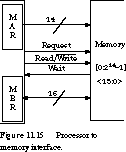
Figure 11.15 shows the processor-memory interface, based on the scheme
introduced in Section 11.1.4. The memory data bus and memory address bus
are 16 bits and 14 bits wide, respectively.
The processor's instructions are:
[XXX] --> AC;
[XXX];
+ Memory[XXX] -->
AC;
= 1 THEN XXX --> PC;
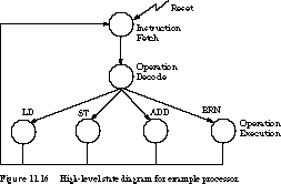
Figure 11.16 gives a high-level state diagram for the processor's control.
This is the starting point for deriving the detailed state machine in this
section. You shouldn't be surprised that its major components are the familiar
sequence of instruction fetch, operation decode, and operation execution.
(RES) the first state. This
starts the machine in a known state when the reset signal is asserted. Also,
it provides the place in the state diagram from which a control signal can
be asserted to force parts of the data-path to known starting values. Perhaps
the most important register to set at Reset is the program counter. In our
machine, we will set the PC to 0. The Memory Request line should also be
driven to its unasserted value on start-up. (RES)
is followed by a sequence of states to fetch the first instruction from
memory (IF0, IF1, IF2). The PC is moved to the
MAR, followed by a memory read sequence. Revising the Moore machine state
fragment of Figure 11.7, we obtain the four-state Mealy sequence shown in
Figure 11.17. 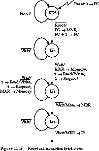
Let's examine the control signals on a transition-by-transition
basis. When first detected, the external reset signal forces the state machine
into state RES. This state resets the PC and Memory Request signals. It
does so by the explicit operation 0 --> PC for resetting the PC on entry
to RES; Request is unasserted because it is not otherwise mentioned. We
assume that register transfer operations not listed in a transition are
implicitly left unasserted.
Once the Reset signal is no longer asserted, the machine
advances to state IF0. On this transition, the control signals to transfer
the PC to the MAR are asserted. This is as good a place as any to increment
the PC, setting it to point to the next sequential instruction. You should
remember that register transfer statements are not like statements in a
conventional programming language. The PC increment takes place on the same
clock edge that causes the MAR to be loaded with the old value of the PC.
Assuming edge-triggered devices, the setup/hold times and propagation delays
guarantee that the old value of the PC is transferred to the MAR. We will
reexamine these timing considerations in the next sub-section.
Figure 11.7 showed that the four-cycle handshake with
memory can begin only when the memory Wait signal is asserted. So we loop
in state IF0 until this Wait is asserted.
Once memory is ready to accept a request and Wait is asserted,
we can begin a read memory sequence to obtain the instruction. On the transition
to state IF1, we set up control signals to gate the MAR to the Memory Address
Bus and assert the Read and Request signals.
Once we have entered IF1, the instruction address has
been presented to memory and a memory read request has been made. As long
as the Wait signal is asserted, these must remain asserted.
We advance to state IF2 when memory finally unasserts
Wait, signaling that data is available on the Memory Databus. On this transition
it is safe to transfer the values on the memory bus into the MBR. This transition
also unasserts the Request signal, indicating to memory that the processor
is ready to end the memory cycle. The four-cycle handshake keeps us in this
state until the Wait signal is again asserted. On this exit transition,
the MBR can be transferred to the IR to begin the next major step in the
state machine: operation decode.
Operation Decode Because of the
simplicity of our instruction set, the decode stage is simply a single state
that tests the op code bits of the instruction register to determine the
next state. This is shown in Figure 11.18.
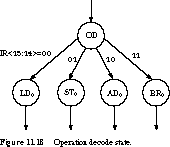
The notation on the transitions from state OD indicates a conditional
test on IR bits 15 and 14. For example, if IR<15:14> =
00, the next state is LD0.
Instruction Execution: LOAD Now
we examine the execution sequences for the four instructions, starting with
LD. The load execution sequence is given in Figure 11.19.
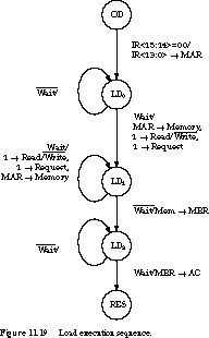
The transition is taken to state LD0 if the op code bits of the IR are
both 0. On this transition, we transfer the address portion of the IR to
the MAR. States LD0, LD1, and LD2 are almost identical to the instruction
fetch states, except that the destination of the data from memory is the
AC rather than the IR. The rationale for the state transitions is also identical:
When memory is ready, we assert Read and Request and keep these asserted
until Wait is unasserted. At this point, the data is latched into the MBR
and then moved to the AC.
Instruction Execution: STORE The
store execution sequence is shown in Figure 11.20. In essence, it is a memory
write sequence that is similar to the load's read sequence. On the transition
from the decode state, the address portion of the current instruction is
transferred to the MAR while the AC is moved to the MBR. If memory is ready
to accept a new request, we begin a write cycle by gating MAR and MBR to
the appropriate memory buses while asserting ![]() and Request. These
signals remain asserted until Wait is unasserted. At this point, the processor
resets the handshake and waits for the memory to do the same.
and Request. These
signals remain asserted until Wait is unasserted. At this point, the processor
resets the handshake and waits for the memory to do the same.
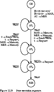
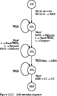
Figure 11.21 shows the execution sequence for the ADD instruction. The
basic structure repeats the load sequence. Only the transition from state
AD2 back to the reset state has a slightly different transfer operation.
Instruction Execution: BRANCH NEGATIVE
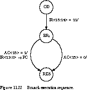
Figure 11.22 gives the final execution sequence, for the Branch if AC
Negative instruction. If the high-order bit of AC is 1, the IR's address
bits replace the contents of the PC. Otherwise the current contents of the
PC, already incremented in the previous RES-to-IF0 transition, determine
the location of the next instruction.
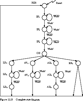
Simplification of the State Diagram Since
the instruction fetch sequence already checks whether memory is ready to
receive a new request by verifying that Wait is asserted, we can eliminate
state ST2. For the same reason, we can eliminate the ![]() loop/Wait exit
of states LD2 and AD2. Similarly, since the IF2 state completes the processor-memory
handshake, we can eliminate the loop back and exit conditions for states
LD0, ST0, and AD0. Figure 11.23 gives the complete state diagram, but does
not show the detailed register transfer operations.
loop/Wait exit
of states LD2 and AD2. Similarly, since the IF2 state completes the processor-memory
handshake, we can eliminate the loop back and exit conditions for states
LD0, ST0, and AD0. Figure 11.23 gives the complete state diagram, but does
not show the detailed register transfer operations.
At this point in our refinement of the state machine,
the list of control inputs and outputs is as follows.
+ 1 --> PC
+ MBR --> AC
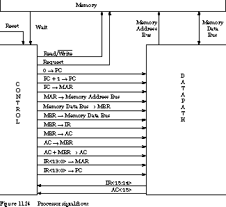
Figure 11.24 gives a revised block diagram showing the flow of signals
between the control, data-path, and memory.
(Load, Store, Add, Branch) or
stage (Fetch, Decode, Execute) that makes use
of the path. (or infrequently) used in the same state.
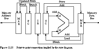
The Store and Add paths between the ALU, AC, and MBR can be combined
as well, yielding the three-bus architecture of Figure 11.26. This is almost
identical to the data-path of Figure 11.13.
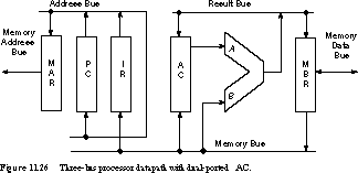
With this organization we can implement the transfer
operation AC + MBR --> AC in a single state. Otherwise
we would need to revise the portion of the state diagram for the ADD execution
sequence to reflect the true sequence of transfers needed to implement this
-operation.
In Figure 11.26 the AC is the only register connected
to more than one bus (it can be loaded from the Result Bus
or the Memory Bus). This is called a dual-ported configuration,
and it requires additional hardware. It is useful to try to reuse existing
connections whenever possible. By using an ALU component that has the ability
to pass its B input through to the output, we can implement the
load path from the MBR to the AC in the same manner as the add path. We
simply instruct the ALU to PASS B rather than ADD A and
B. This yields the three-bus architecture introduced in Figure
11.13, eliminating the extra data-path complexity associated with a dual-ported
AC. We assume this organization throughout the rest of this subsection.
Implementation of the Register Transfer Operations Now
that we have settled on the detailed connections supported by the data-path,
we are ready to examine how register transfer operations are implemented.
A data-path control point is a signal that causes the data-path
to perform some operation when it is asserted. Some control operations,
such as ADD, PASS B, 0 --> PC, PC + 1 -->
PC, are implemented directly by the ALU and PC functional units. For other
operations, such as PC --> MAR, we have to assert more than one control
point within the data-path. These more detailed control signals are often
called microoperations. Thus, we can decompose a register transfer
operation into one or more microoperations, and there is one microoperation
for each control point (for example, a register load or tri-state
enable control input) in the data-path.
As an example, let's examine the register transfer operation
PC --> MAR. To implement this, the PC must be gated to the Address Bus
while the MAR is loaded from the same bus. In terms of microoperations,
PC --> MAR is decomposed into PC --> ABUS and ABUS --> MAR.
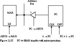
Figure 11.27 shows how these operations manipulate control points in
the data-path. The PC is a loadable counter, attached to the ABUS via tri-state
buffers. The MAR is a loadable register whose parallel load inputs are driven
from the ABUS. Asserting the microoperation PC --> ABUS connects the
PC to the ABUS. Asserting the ABUS --> MAR microoperation loads the
MAR from the ABUS.
Timing of Register Transfer Operations
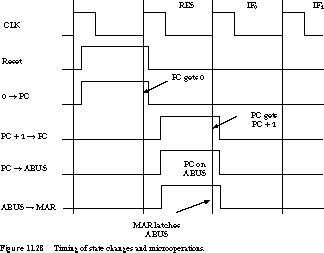
Figure 11.12 shows the timing for these signals. The waveform begins
with entering state RES, followed by advancing to state IF0. In this timing
diagram we assume the Reset signal is debounced and synchronized with the
system clock and 0 --> PC is directly tied to the synchronized Reset.
We use positive edge-triggered registers and counters with synchronous control
inputs throughout. Although we assume positive logic in this timing diagram,
you should realize that most components come with active low control signals.
The Reset signal is captured by a synchronizing flip-flop
on the first rising edge in the figure. A propagation delay later, the synchronized
version of the reset signal is presented as an input to the control. No
matter what state the machine is in, the next state is RES if Reset is asserted.
The 0 --> PC microoperation is hardwired to the synchronized Reset signal.
The synchronous counter CLR input takes effect at the next rising edge.
This coincides with the transition into state RES.
Once we are in state RES, we assume that the Reset input
becomes unasserted. Otherwise we would loop in the state, continuously setting
the PC to 0 until Reset is no longer asserted. With Reset unasserted, IF0
is the next state and the microoperations PC + 1 --> PC,
PC --> ABUS, and ABUS --> MAR are asserted.
Because of the way they are implemented in the data-path,
some of these operations take place immediately while others are delayed
until the next clock edge/entry into the next state. For example, asserting
PC --> ABUS turns on a tri-state buffer. This takes place immediately.
Microoperations like PC + 1 --> PC (counter
increment) and ABUS --> MAR (register load)
are synchronous and therefore are deferred to the next clock event.
In the waveform, soon after entry into RES with Reset
removed, we gate the PC onto the ABUS. Even though the PC count signal is
asserted, it will not take effect until the next rising edge, so the ABUS
correctly receives 0.
On the next rising edge, the MAR latches the ABUS and
the PC is incremented. Because the increment propagation delay exceeds the
hold time on the MAR load signal, the 0 value of the PC is still on the
ABUS at the time the load is complete. When a bus is a destination, the
microoperation usually takes place immediately; if a register is a destination,
the microoperation's effect is usually delayed.
Tabulation of Register Transfer Operations and
Microoperations The relationships between register transfer
operations and microoperations are:
Some of these operations can be eliminated because
a connection is dedicated to a particular function and thus does not have
to be controlled explicitly. AC --> ALU A and ALU Result --> RBUS
are examples of this, since the AC is the only register that connects to
ALU A and the ALU Result is the only source of the RBUS.
This leads us to the revised microoperation signal flow
of Figure 11.29.
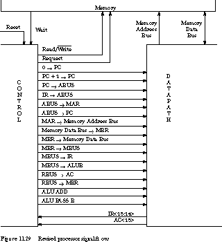
Two control signals go to memory, Read/![]() and Request, and
16 signals go to the data-path. The control has a total of five inputs:
the two op code bits, the high-order bit of the AC, the memory Wait signal,
and the external Reset signal. It is critical that the latter two be synchronized
to the control clock.
and Request, and
16 signals go to the data-path. The control has a total of five inputs:
the two op code bits, the high-order bit of the AC, the memory Wait signal,
and the external Reset signal. It is critical that the latter two be synchronized
to the control clock.
[Top] [Next]
[Prev]